Active Receiving Antenna AAK 5240
Die AAK 5240 ist ein Aktivantenne, welche von der Fa. DUK vertrieben wurde.
Sie können auf der Firmenhomepage weitere Informationen sehen.
Bitte die Adresse nutzen ( kein Link )
Fa. AAS
active-receiving-antennas/dipoles-horizontally-polarized/64-aak-5200
DUK Active Receiving Antenna AAK 5240
Discription of Types - AAK 5 2 4 0
Type of Antenna ( 5 )
5 = two dipoles ( two autputs ) - with / without Monopole
Frequency Range – Dipoles ( 2 )
2 = 1.5 – 30 Mhz
Frequency Range – Monopoles ( 4 )
4 = 0.01 – 30 Mhz
Rods and Modifications ( 0 )
0 = with detachable rod ( standard version
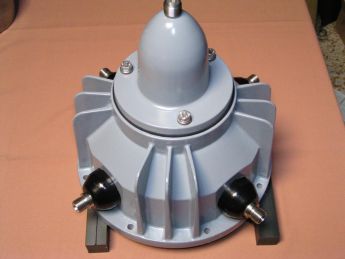 AAK 5240 - 10 khz bis 30 MHz
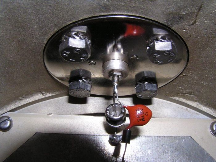 Dipol Anschluss mit Überspannungsableiter
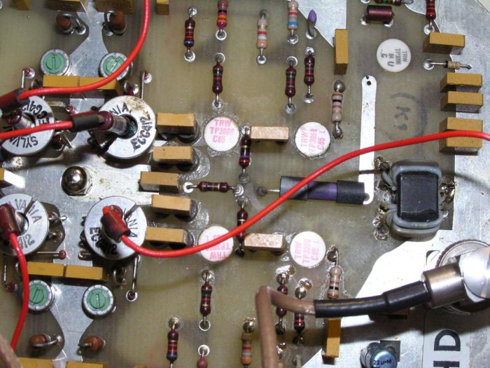 aktive Bauteile
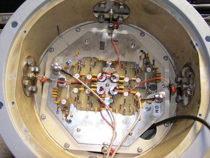 Gehäuse von unten geöffnet
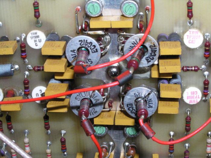
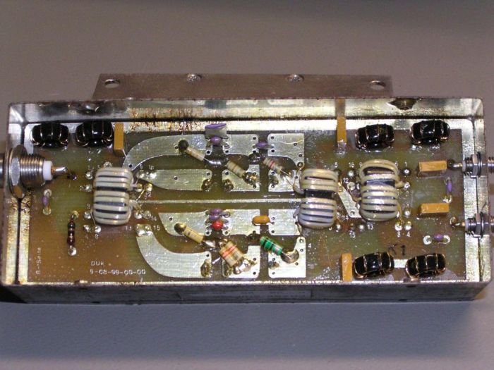 Phasenschieber
 Phasenschieber detail
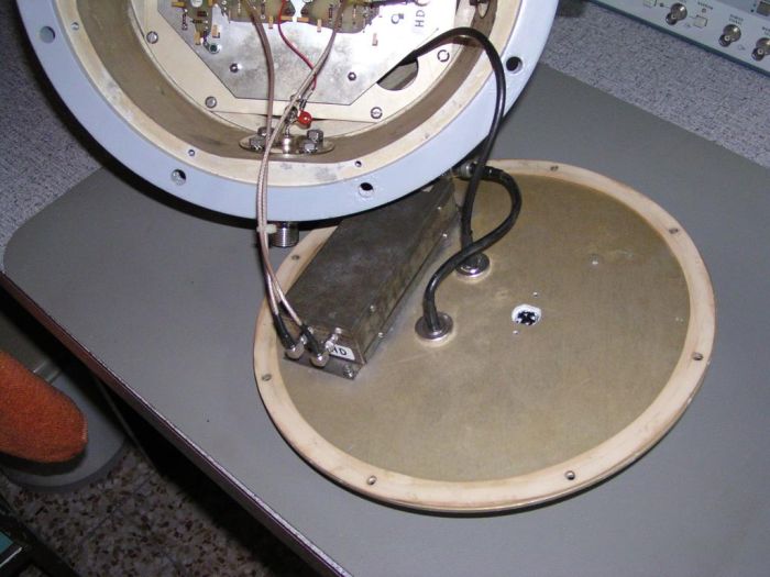 Phasenschieber im Weisblechgehäuse
AAK 5240 Construction
The antenna amplifiers for the horizontal dipoles are installed in a watertight, seawater resistant eloxal coated Aluminium alloy housing, the antenna head. The antenna rods are made of glassfibre reinforced plastics fitted with stainless steel screw connections.
The vertical antenna is electricaly independent from the dipoles. Its amplifier is housed in the cavern of a separate base insulator of compression moulded glassfibre reinforced plastics. It may be installed onto the top of the cast aluminum head.
The cable connectors are fitted to the underside of the antenna head's bottom flange.
Cable diagram
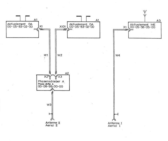
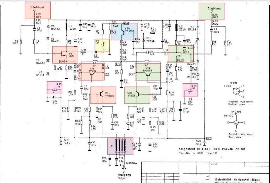
Circuit diagram - Horizontal
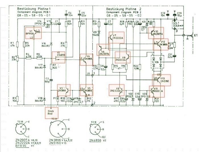
Circuit diagram - Vertikal
Circuit discription - Horizontal Dipole
The aktive part of the horizontal dipole is made of a differential amplifier which contains transistors V1, V12, and V14 on the one side and V2, V13, and V15 on the other side.
The transistor V16 supplies a constant current of 180 mA to the differential amplifier. This current is divided equally such the initial current of 90 mA flow through each of the two arms of the differential amplifier.
The transformer T1 sums up the alternating current of the collectors of transistors V14 and V15 in proper phase relation. The secondary of the transformer delifers the RF – Signal into 50 Ohms. As the supply voltage for the active element travels along the coaxial cable the transformer T1 also separates the dc from the radio Signal.
The active element must be protected against too high input voltages as they happen, for exemple, to appear during a near-by lightning strike.
A three-stage overload protection is applied to each connection between the passive and the active antenna parts. This overload protection comprises an air gap discharger, a glow discharge gas tube and negative biased diodes V3 – V6 and V7 – V10.
Omnidirectional receiving in the horizontal pattern is archieved by means of a 90° phase shifter wich combines the outputs of the two dipoles. Tha phase shifter is bridged by the chokes L1 – L6 in order to supply the dc voltage to the amplifiers.
Circuit discription - Vertical Antenna
The RF signal produces by the antenna rod passes a spark arrester to bypass static charges, and is applied to the gate of field-effect transistor V2 via coupling Capacitor C2 and protecting resistor R7. The gate bias voltage of this transistor is determined by resistors R1 through R3. In order to maintain a high – impedance input, the bias voltage is applied to the gate by resistors R4 and R6. The reverse biased diodes V15 through V18 protect the input of the FET.
Transistor V1 provides a bias regulation for the field-effect transistor at high input voltages. The 20 mA drain current through V2 is established by transistor V3,
wich operates as a constant currend source. Field-effect transistor V2 operates as a source follower.
Its RF output signal is applied to the base of transistor V4, wich operates as an emitter follower with its emitter quiescent curred of approx. 30 mA determined by V5.
From the emitter of transistor V4 the Rf signal is feed to the base of output transistor V13 and – via – C6 – to the base of output transistor V12. From the common emitter point of the transistors V12 and V13 the signal is coupled to the coaxilal cable by C11 and R23.
Choke L1 blocks the dc path for RF voltages. Diode quad V24 together with transistors V6 through V11 with their associaded circuitry form a regulator circuit controlling temperature behaviour and cross modulation properties of the output stage.
The quiescent currend of the output stage amounts to approx. 18MA, and is given by V10 and V11. The supply voltage for the active circuit of the antenna is 38 Volt dc. The dc supply current under no – signal conditions is approx. 100 mA